


3-in-1 Alternative Energy Car DIY STEM Kit
$19.99$14.95
Posted on: Feb 3, 2004
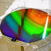
Photo courtesy: Ralf Heilmann
An MIT device that makes the world’s most precise rulers—with "ticks" only a few hundred billionths of a meter apart—could impact fields from the manufacture of computer chips to space physics.
The Nanoruler is 10 to 1,000 times faster and more precise than other methods for patterning parallel lines and spaces (known collectively as gratings) across large surfaces more than 12 inches in diameter. Such large surfaces are key to a number of applications involving gratings, such as larger wafers for the production of computer chips and higher-resolution space telescopes.
"Patterning gratings with precise control across large areas has bedeviled labs around the world for a long time, despite great efforts," said Mark L. Schattenburg (Ph.D. 1984), leader of the team and director of MIT’s Space Nanotechnology Laboratory in the Center for Space Research (CSR).
The Nanoruler can pattern gratings of lines and spaces separated by only a few hundred nanometers, or billionths of a meter, across a surface 300 millimeters in diameter. It does so with a precision of less than one nanometer. "That is the equivalent of shooting a target the size of a nickel in Manhattan all the way from San Francisco," said Carl G. Chen (Ph.D. 2003), one of Schattenburg’s colleagues.
The researchers reported the results of initial trials of the Nanoruler in the November-December issue of the Journal of Vacuum Science and Technology B. In addition to Schattenburg and Chen, they include Paul T. Konkola (Ph.D. 2003) and CSR research scientist Ralf K. Heilmann. The team also received significant technical assistance from Robert Fleming of the CSR sponsored research technical staff.
The Nanoruler continues a line of research in advanced grating fabrication technology initiated at MIT in the late 1940s. Gratings are of particular interest to scientists and engineers because, among other things, they allow the analysis of light.
When the distance between one line and its neighbor, or period, is comparable to the wavelength of light, a phenomenon called diffraction occurs. Essentially the grating spreads the light into a spectrum, much as a prism spreads light into its colors. That spectrum, in turn, can be analyzed for information about the source.
For example, one such grating is key to NASA’s Chandra X-ray Observatory. The High Energy Transmission Grating, also developed by Schattenburg’s lab at MIT, spreads the X-rays from Chandra’s mirrors into a spectrum that can then be "read" like a kind of cosmic bar code. From there, scientists can deduce the chemical composition and temperature of the source (such as the corona of a star).
BUILDING A BETTER RULER
Schattenburg began the Nanoruler project because he wanted to create a better ruler for the semiconductor industry. "Today’s advanced computer chips are packed with millions of transistors," he said. "Increasingly, however, it becomes a challenge to stuff more and more of these ever-shrinking features into an area no larger than a thumbnail."
What Schattenburg wanted, in essence, was an extremely well-made ruler whose ticks are spaced not millimeters but nanometers apart, and whose size was comparable to the largest commercial silicon wafers. "If such a ruler could be created, it would help chip makers do a much better job of laying down the Lilliputian circuitry," he said.
The Nanoruler does the trick by combining two conventional methods to create gratings: mechanical ruling and interference lithography. Mechanical ruling essentially involves dragging a very sharp tool—almost always a diamond point—across the surface to form the sets of lines and spaces. Among other drawbacks, however, it is time-consuming.
In interference lithography, two beams of light interfere with each other to produce interference "fringes," or parallel planes of high and low light intensity. These fringes can then be recorded in the surface as lines and spaces, using the same techniques common to the patterning of miniscule designs on computer chips. Interference lithography is much faster than mechanical ruling since all the grooves are formed simultaneously in a single exposure.
The Nanoruler essentially moves the surface to be patterned on a stage as a laser creates the interference fringes that in turn become the lines and spaces. "While other tools can make gratings with smaller periods, none is as fast or as accurate as the Nanoruler," Schattenburg said. The project, which took five years, has had its share of trials and tribulations, Chen recalls. For example, toward the end he was stuck in Beijing for six months due to a visa delay. During that time he was able to work out some of the fundamental physics validating the Nanoruler concept.
"The experience of building the Nanoruler from scratch has been immensely rewarding," he concluded.
NASA and DARPA sponsored the research. The Nanoruler is patent-pending. For more information, go to http://snl.mit.edu.


