


Solar + Battery Car DIY STEM Kit
$11.99$6.95
Posted on: Jan 6, 2004
The discovery of carbon nanotubes heralded a new era of scientific discovery that included the promise of ultra-sensitive bomb detectors and super-fast computer memory chips. But finding a way to incorporate nanomaterials into a working nanoelectronic system has been a frustratingly elusive achievement - until now.
In an important milestone in the fields of nanosciences and nanoengineering, researchers at the University of California, Berkeley and Stanford University are announcing that they have created the first working, integrated silicon circuit that successfully incorporates carbon nanotubes in its design.
"Until our work, no group has publicly reported success in directly integrating nanotubes onto silicon circuits," said Jeffrey Bokor, UC Berkeley professor of electrical engineering and computer sciences and principal investigator of the project. "It is a critical first step in building the most advanced nanoelectronic products, in which we would want to put carbon nanotubes on top of a powerful silicon integrated circuit so that they can interface with an underlying information processing system."
Researchers say the development brings them a significant step closer to using carbon nanotubes for memory chips that can hold orders of magnitude more data than current silicon chips - 10,000 times greater, according to some estimates - or for sensors sensitive enough to detect traces of explosives or biochemical agents at the molecular level.
UC Berkeley engineers teamed up with chemists at Stanford to develop an integrated circuit that can dramatically speed the analysis of thousands of synthesized carbon nanotubes. The description of this work appears in the January 2004 issue of Nano Letters, a publication of the American Chemical Society.
"These results represent a dream come true," said Hongjie Dai, associate professor of chemistry at Stanford and co-principal investigator of the project. "This achievement opens up a vast number of possible applications in nanotechnology."
A carbon nanotube, which looks like rolled chicken wire when examined at the atomic level, is tens of thousands of times thinner than a human hair, yet remarkably strong. It has attractive electrical properties, which several research groups - including the one led by Dai at Stanford - have harnessed to create high performance transistors.
The road to creating the first nano-silicon hybrid circuit began as a solution to a practical research problem: How to refine the process of growing nanotubes so that they are created with predictable qualities.
Depending on the molecular structure specific to each carbon nanotube, it can either be metallic and capable of conducting electricity, or act like semiconductors, with conductivity that can be turned on and off. But the current synthesis process results in an unpredictable proportion of metallic and semiconducting nanotubes, leaving researchers uncertain as to how much of each type they'll get in any one batch.
Analyzing whether a batch yielded metallic or semiconducting nanotubes involved a labor-intensive processing of manually checking the electrical conductivity of each carbon nanotube.
To resolve this problem, the researchers set out to build a device that would automate the process of decoding thousands of carbon nanotubes on a silicon chip. Working with UC Berkeley's Microfabrication Laboratory, they created a chip with silicon metal oxide semiconductor (MOS) circuitry. The chip, dubbed the random access nanotube test chip, or RANT, contains a network of silicon wires and switches that form a circuit.
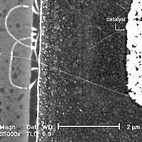
Researchers then proceeded to grow carbon nanotubes directly onto "islands" on the circuit platform that contained the necessary catalyst for nanotube synthesis. The extreme heat required to grow nanotubes would typically melt the circuitry of traditional semiconductors, but the researchers got around that problem by interconnecting the silicon transistors with molybdenum, a refractory metal that can withstand very high temperatures.
"We first envisioned a patterned growth of carbon nanotubes on silicon wafers five years ago, but it wasn't clear at that time whether that approach would work as an integrated nanotube-silicon hybrid circuit," said Dai. "It was the combined expertise in chemistry, materials science and electrical engineering that made this a reality."
The resulting chip contained thousands of carbon nanotubes connected to the circuit on a 1-square-centimeter silicon chip. By turning certain switches on and off, researchers were able to isolate the path that leads to an individual nanotube. Not only could researchers pinpoint which nanotube was responding to electrical current passing through the system, they could tell whether the conductivity could be turned on or off. If they were able to change the conductivity of the nanotube, they knew that it was a semiconductor and not metallic.
"The circuit is interconnected in such a way that only 22 control signals are needed in testing more than 2,000 nanotubes," said Yu-Chih Tseng, a UC Berkeley graduate student in electrical engineering and computer sciences and lead author of the paper. "The key is that this can all be done by a machine and computer.
We succeeded in making a tool for nanotechnology researchers, and in the process, we demonstrated the broader proof of principle that nanotubes can be successfully integrated in a complex circuit."
Research such as this is an important component of the UC Berkeley-based Center for Information Technology Research in the Interest of Society, or CITRIS. The center includes a major emphasis on nanosciences and nanoengineering, and is funding the construction of a new nanofabrication laboratory on the UC Berkeley campus that would significantly enhance researchers' ability to conduct such fundamental and innovative work, said Ruzena Bajcsy, director of CITRIS.
Bokor cautions that the integrated circuit they have built is not a likely candidate for commercialization just yet. For one, the molybdenum they used to protect the circuit from heat damage is not a typical material used in the semiconductor industry because it is a high-resistance metal.
Nevertheless, the achievement opens the door for other promising research on nanotechnology devices, including those made of silicon nanowires and organic polymers, researchers said.
"Carbon nanotubes have fascinated many scientists and those interested in science ever since they were discovered," said Ali Javey, a graduate student in chemistry at Stanford and co-author of the paper. "This work takes us an important step forward by proving the compatibility of the nanotube synthesis process with modified silicon technology and leading the way to future nanotube-based commercial applications."
The research was conducted as part of the Materials, Structures and Devices Center, one of five multi-university focus centers funded by the Microelectronics Advanced Research Corporation (MARCO), a subsidiary of the Semiconductor Research Corporation. The project was also supported by the Defense Advanced Research Projects Agency (DARPA).
Other co-authors of the study include Peiqi Xuan and Ryan Malloy at UC Berkeley, and Qian Wang at Stanford.


