


Fan Micro Car DIY STEM Kit
$9.99$5.55
Posted on: Jun 17, 2003
Click here for a larger image.
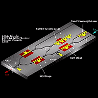
A research team at the University of California at Santa Barbara (UCSB) has for the first time incorporated on a single chip both a widely tunable laser and an all-optical wavelength converter, thereby creating an integrated photonic circuit for transcribing data from one color of light to another. Such a device is key to realizing an all-optical network. This research is being funded by a Defense Advanced Research Projects Agency (DARPA) Microsystems Technology Office (MTO) grant to push the boundary for photonic-circuit functional integration.
Think about data transmission over the Internet in terms of a telephone call between Los Angeles and New York. What enables two people to talk is the 'dedicated' line between them. On the Internet the long-distance transport of information between the two cities is via optical fibers or light pipes, which can move numerous colors of light over a single fiber at the same time with each color representing a 'dedicated' line for the transmission of data (i.e., wavelength division multiplexing [WDM]).
Data moves between coasts through nodes of the Internet located in cities like Phoenix or Houston, where the capability is needed to switch information arriving on one fiber as orange photons to continue the next leg of their journey on another fiber as red photons because the channel for orange on that fiber is in use. Today, this switching from one color to another has to be done by converting photons to electrons, switching electronically, and converting electrons back to photons.
The new postage-stamp-size device is a tunable 'photon copier,' which eliminates electronics as the middleman.
It is as if information on orange paper were being copied onto red paper. The information stays the same, but the color of the paper on which it is conveyed is different. By that analogy the tunable laser supplies the red paper, and the wavelength converter functions as the copy-machine transcribing the information of the orange original to red. The tunable laser is able to supply a wide range of colors and hues to copy onto, and the wavelength converter is able to maintain or improve the quality of the image, a process called 'regeneration.'
Past attempts to engineer photonic circuits with tunable lasers and wavelength converters have met with limited success, and the two components have heretofore lived on separate chips. Fabricating them on the same indium phosphide platform and thereby integrating them represents a technological breakthrough and greatly enhances performance and commercial feasibility. Integration provides many benefits, which include, notably, maintaining the quality of the signal by avoiding the taking of light on and off the chip many times.
In electronics, one semiconductor component incorporating two capabilities typically costs much less than half of what two separate components, each supplying one of those capabilities, costs. Photonics requires breakthroughs to follow these same laws of integration.
Daniel Blumenthal, leader of the research group and a UCSB professor of electrical and computer engineering, figures this successful demonstration of two capabilities on one photonic chip means more to come. 'People are now accustomed,' he said, 'to think of a silicon substrate with a seemingly innumerable number of transistors on it. But that sophisticated electronic technology of today began back in the 1960s with a couple of transistors, and photonics is just beginning to enter that stage. We have been working long and hard at cracking this problem, and we are finally at the demonstration phase.'
UCSB graduate student Milan Masanovic presented the findings (in a paper entitled 'Demonstration of Monolithically-Integrated InP Widely-Tunable Laser and SOA-MZI Wavelength Converter') at the 15th annual meeting of the Indium Phosphide and Related Materials Conference, held in May in Santa Barbara. That presentation earned him the conference Best Student Paper Award.
The paper states, 'The monolithic integration of tunable lasers and all-optical wavelength converters is a critical step towards realizing truly optical switches and networks. These structures allow data to be imprinted from an input wavelength to a tunable output wavelength without passing the signal through electronics.'
Masanovic is a student jointly of Blumenthal and the paper's other faculty author and research team co-leader, Larry Coldren, who is the inventor of the tunable laser used in this device, which is called a Sampled-Grating Distributed-Bragg-Reflector laser (SGDBR). A 'tunable' laser enables the dialing up of different colors (i.e., a single miniscule device can be programmed to emit at one frequency and then re-programmed to emit at another by electronically changing the effective optical length of its cavity and the shape of its internal color filter).
The all-optical wavelength converter is an SOA-based Mach-Zehnder interferometer (SOA-MZI), which the paper's authors note 'also implements the significant feature of digital signal regeneration.' Digital regeneration is key to moving optical signals around a network with many nodes and long stretches of fiber in between and is a feature that electronics uses pervasively.
The other three authors on the paper are Blumenthal's graduate student Vikrant Lal and Coldren's students Erik Skogen and Jonathon Barton.
The research is being conducted under the auspices of a four-year, $3.5 million DARPA grant through the Microsystems Technology Office (MTO) Chip-Scale WDM program to investigate how to pipe digital and analog information through a photonic circuit on a single compound semiconductor chip; Dr. Jagdeep Shah is the program manager. Blumenthal, who serves as associate director of the UCSB Multidisciplinary Optical Switching Technology (MOST) Center, is the principal investigator for the grant. The other four UCSB researchers are all professors of electrical and computer engineering: Coldren, director of the Optoelectronics Technology Center (OTC); John Bowers, director of MOST; Evelyn Hu, acting director of the California NanoSystems Institute (CNSI); and Nadir Dagli.


