


Flashing LED Circuit DIY Electronics Kit
$4.99$2.95
Posted on: Sep 14, 2003
Minuscule wires a few nanometers across are proving to be versatile electronic components, as demonstrated recently by University of California, Berkeley, chemists who used silver nanowires as key elements of a sensitive explosives detector.
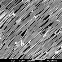
The researchers, led by Peidong Yang, ChevronTexaco assistant professor of chemistry at UC Berkeley and a chemist with the Materials Sciences Division of Lawrence Berkeley National Laboratory, made about a trillion silver nanowires - essentially nanocopic needles - and packed them tightly together in a thin layer, all needles pointing in the same direction, like rafted logs on a river.
The layer of ordered nanowires made an ideal site for chemicals to bind for detection by a very sensitive technique called surface-enhanced Raman spectroscopy.
This nanowire-based sensing scheme could have "significant implications in chemical and biological warfare detection, national and global security, as well as medical detection applications," Yang and UC Berkeley colleagues report in a paper that appears in the Sept. 10 issue of Nano Letters, a publication of the American Chemical Society.
"Raman spectroscopy is an extremely sensitive and specific technique that basically gives you a chemical signature, a fingerprint," Yang said. "A monolayer of silver nanowires makes a very sensitive substrate on which to detect molecules like DNT (dinitrotoluene, a cousin to TNT), which is used in making essentially all explosives, including land mines. Those explosives have DNT vapor coming out, allowing us to do airborne detection."
Yang said that the packed silver nanowires are a better surface for enhanced Raman spectroscopy than a thin layer of silver because the nanowire surface is more ordered and gives a more clearly defined signal, making interpretation of the Raman vibrational spectrum easier. The packed silver nanowires are uniform, reproducible and suitable for use in air or in liquid.
He is hoping to miniaturize the laser and other components required by Raman spectroscopy to create a microscopic sensor on a chip, allowing very sensitive and specific detection of chemicals like explosives.
Yang's co-authors include Lawrence Berkeley National Laboratory post-doctoral chemist Christian Hess and UC Berkeley graduate students Andrea Tao and Franklin Kim. Other collaborators are graduate students Joshua Goldberger and Rongrui He of UC Berkeley's Department of Chemistry, and chemists Yugang Sun and Younan Xia of the University of Washington, Seattle.
The nanowire layers have other potential uses, too. Yang said that the monolayers can be transferred to any surface, including silicon, glass or flexible plastic polymers, to provide a large area on which to do chemistry. He and his team were able to make flexible sheets of packed nanowires more than three square inches in area (20 square centimeters).
"You could fabricate these in large areas, providing a flexible monolayer that would be a key component in a number of devices, such as flexible solar cells and light emitting diodes" Yang said.
His lab has created similar flexible layers of packed semiconducting nanowires made of silicon that would also be useful in flexible electronic devices. A group at Harvard University reports a similar development with silicon nanowires in the same issue of Nano Letters.
"These are probably the first two examples of techniques that can do large scale assembly of nanostructures, enabling macroscopic manipulation of lots of them simultaneously," said Yang. "You need this ability to manipulate nanowires or nanotubes if they are to become practical electronic components."
Two years ago Yang proved that optical materials like zinc oxide can form nanowires that act as lasers, and he has succeeded in mating nanowires of different materials to create one-dimensional junctions akin to transistor junctions.
This latest triumph employed a technique whereby nanowires are floated on top of a liquid and then compressed to make the nanowires align and clump together tightly. This old technique, called Langmuir-Blodgett assembly, succeeded in creating monolayers measuring 20 square centimeters in area, which Yang could slip onto a flexible surface such as a plastic polymer. Each silver nanowire is about 50 nanometers across - about the diameter of the polio virus - and 2-3 microns long, with a pentagonal cross section and pyramidal tip.
Monolayers can be layered into stacks of alternating semiconductor (silicon) and conductor (silver) to produce other types of devices, he said.
"With monolayers of metal and monolayers of semiconductor, we can do multilayer transfers and stack up these flexible devices to make flexible composites," he said. "The large-scale assembly process we developed to assemble nanowires over a large area will have a significant impact in the nanoscience/technology field."
The work is funded by the Camille and Henry Dreyfus Foundation, ACS-Petroleum Research Fund, Alfred P. Sloan Foundation, Beckman Foundation, David and Lucile Packard Foundation, U.S. Department of Energy, National Science Foundation and Multidisciplinary University Research Initiative of the Air Force Office of Scientific Research (AFOSR-MURI).


